You are using an out of date browser. It may not display this or other websites correctly.
You should upgrade or use an alternative browser.
You should upgrade or use an alternative browser.
Teensy PCB Ardumower (T-Mow)
- Thread starter Sascha
- Start date
Ok Sascha, in this case, my PCB is like the picture you sent.This was the Schematic on Bernards PCB and the Picture from you is the new.


@Sascha HelloTest of Power PCB V1.06 is OK with ESP8266 3.3V module.
R10 and R11 i use 4.7K . D3 is not mount.
") I also have to do this R10 and R11value change to 4.7K on the PCB Card ? and about R9-R10 / R8-R7, same soldering changes as for R12-R5 / R6-R13 ?
I also have to do this R10 and R11value change to 4.7K on the PCB Card ? and about R9-R10 / R8-R7, same soldering changes as for R12-R5 / R6-R13 ?Thanks Bernard and Sascha, OK for power pcb. Received components from Reichelt todayNö Changes in the powerpcb.
Hi Sascha and Bernard, just to let you know that for 69.90€ it's the charging station and the charger; already ordered.Is it charging station and charger for 69€? I do not know it at all more.
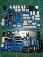
Here a picture:

Yes, for Sensors that need extra PullupsAre J3 and J30 Reserve ?
I'm not sure, think Reserve for Sensorsfor what are J27 and J36 used ?
Many things to do; change 100 Resistors with 010 ones on cards, to solder the condensator, to add pinconnectors on Teensy and esp32 etc... .
Sascha, if you do a next version of Power PCB, could ot be possible to add room between J11/J12 and INA226 card ? I can't connect J11 and J12 without pushing on INA card.
Also, I had to bore larger holes for D2 and D5.
Question: the two connections on INA226 cards with seperated pins shouldn't be connected with stronger pins, with stronger holes in PCB ? (the question also is what could be used in this case... didn't find strongers from Reichelt, with the same distance between both pins).
Don't hesitate to let me know if you see something wrong !
Attachments
Last edited:
Bonjour Laurent et Joyeux noel.R10Many things to do; change 100 Resistors with 010 ones on cards, to solder the condensator, to add pinconnectors on Teensy and esp32 etc... .
Sascha, if you do a next version of Power PCB, could ot be possible to add room between J11/J12 and INA226 card ? I can't connect J11 and J12 without pushing on INA card.
Also, I had to bore larger holes for D2 and D5.
Question: the two connections on INA226 cards with seperated pins shouldn't be connected with stronger pins, with stronger holes in PCB ? (the question also is what could be used in this case... didn't find strongers from Reichelt, with the same distance between both pins).
Don't hesitate to let me know if you see something wrong !
Sur les photos je vois ceci:
Power PCB:
Q3 ne semble pas etre dans le bon sens.
J2 J3 J11 J12 il vaut mieux les souder dans l autre sense (comme vous l avez fait pour J9 et J10.)
Main PCB.
Diode D7 et D8 :
D7 sert a eviter une inversion dans le + et - du connecteur J25 ,donc si vous faites attention elle n'est pas utile. Si vous l'utilisez vous devez penser qu'il y a une chute de tension a ses bormes et donc vous devez avoir (5V a la SORTIE de D7 en reglant le DC/DC XL4015 ), soit certainement 5.2 V ou plus a J25.
D2 et R11 ne servent a rien ,il est preferable de ne pas les connecter (en effet lorsque le PCB est alimenté il y a deja une led sur l'ESP32 et sur le GY-521 qui nous assure de la presence de tension sur le PCB et cela evite de surcharger le convertissuer DC/DC du teensy).Lors des premiers tests ,j'avais un doute sur la puissance du convertisseur DC/DC du teensy qui genere le 3.3V a l'ensemble des peripherique du PCB (c'est pourquoi la presence de J29 et JP1 , mais apres les tests il n'est pas nécessaire d'avoir plus de puissance sur le 3.3V du PCB et donc J29 est inutile D8 inutile et JP1 toujours a gauche ATTENTION il n'est pas present sur votre photo)
N'oubliez pas de couper le shunt sur le teensy4.1 si vous alimentiez le PCB par J25 et avez le cable USB connecté a votre PC en meme temp.
et sutout regler le DC/DC XL4015 pour avoir 5V a la sortie de D7 avant de connecter l'ESP32,le Teensy et le GY-521.
R7 R8 R9 R10 je ne sais pas les changements que @Starsurfer78 a fait sur le schema, il faut donc verifier comment tout est relié . Avez vous le plan exact de votre PCB.
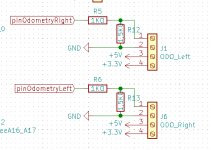
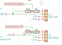
R5 R6 R12 R13 sont a adapter en fonction du type d'odometry que vous allez utiliser et vérifier le plan pour etre certain de ne jamais avoir plus de 3.3V sur une des entrées du TEENSY.
Last edited: