If i understand correctly the issue:
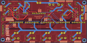
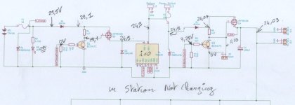
With nothing on PCB (no ina226),nothing on J2 and J5(no 3.3V)
J6 is shunt and J9 is open ,Each time you connect the battery you have 24V on J11 or J12 ??
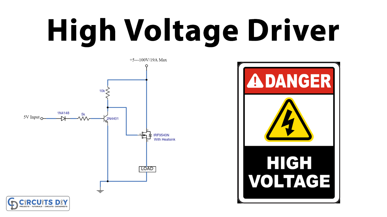
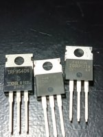
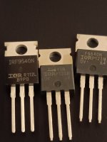
If Yes you need to first try to remove (unsolder) Q3 to see if it's change something ,if no then Q4 is not OK or destroy or no in correct orientation.
Standard working mode is:
When battery is plug, you have 24V on J11 only when you shunt J9 and 0V when release.
When you shunt J9 --> 24V on J11 --> main PCB start and send back 3.3V on J5 Batteryswitch, so Q3 is close and you can release J9 to have the power on state , If main PCB stop to send 3.3V on J5 Batteryswitch J11 is back to 0V and everything is OFF.
3.3V on J5 chargeenable ---> start the charging process.

